


EEE 120
Lab 1 Answer Sheet (Online)
Half Adder, Full Adder, 4-bit Incrementer and Adder
Name: ______________________________________
Date: _______________________________________
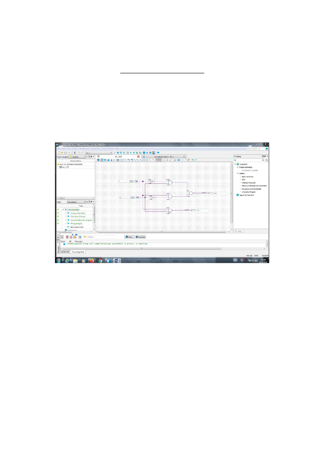
Task 1-1: Build and Test the 1-Bit Half-Adder
Include a picture of your Quartus circuit here:
Please comment on the single biggest issue you were facing when designing the circuit.
Include a picture of your Quartus simulation (timing diagram) here:
1
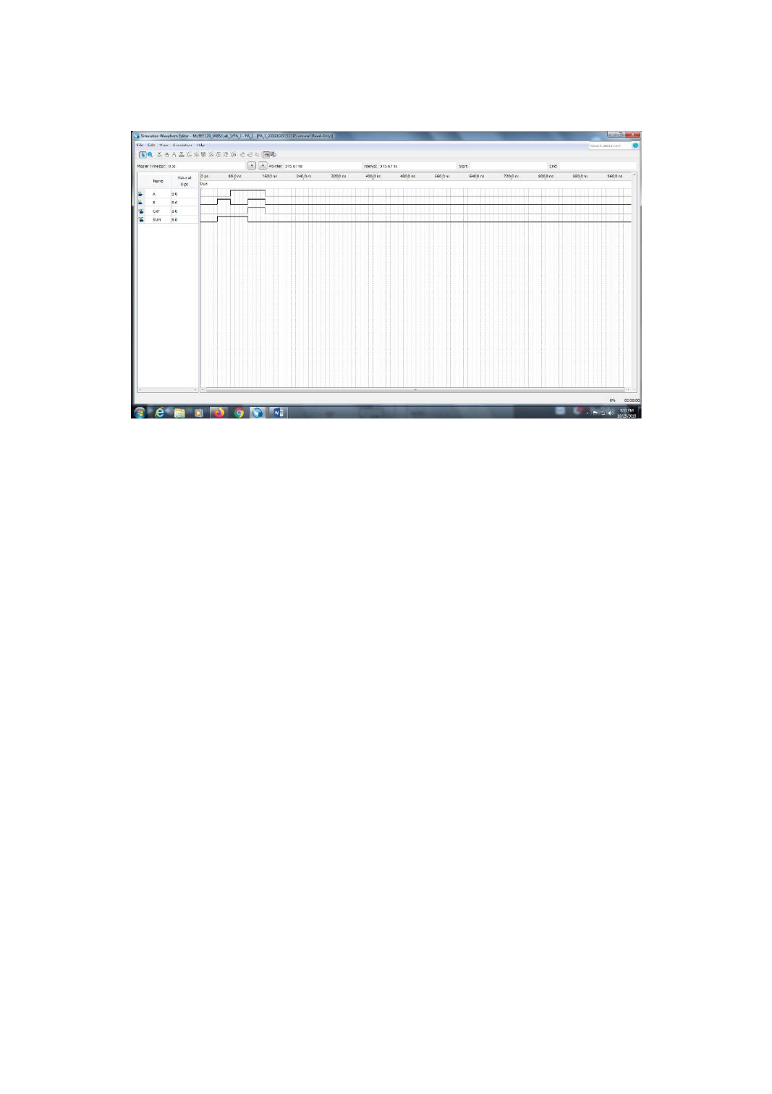
Did the circuit behave as expected? If no, what was wrong? – Yes (eventually)
Please comment on the single biggest issue you were facing when simulating the circuit.
Issue: When I attempted to run the analysis and synthesis, I received errors. I named my inputs “input
A” and “input B”, that was not allowed. I renamed them A & B and then it worked.
Task 1-2: Build and Test a 4-Bit Increment Circuit
Include a picture of your Quartus circuit here:
2
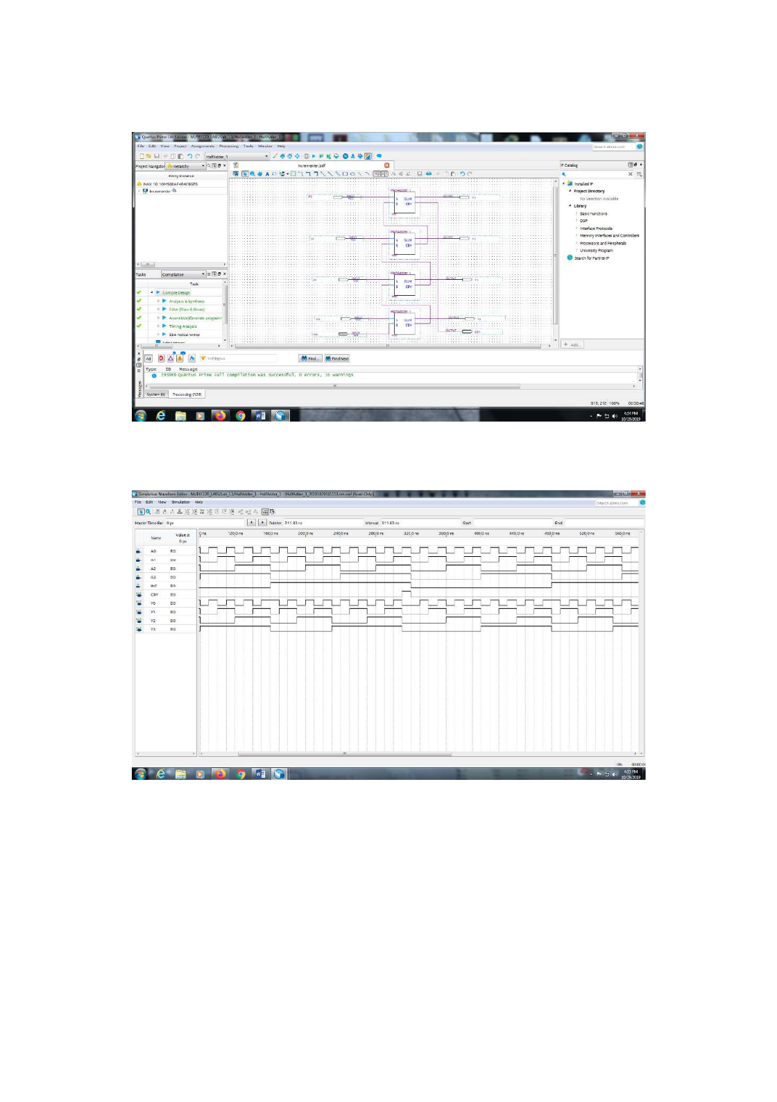
Please comment on the single biggest issue you were facing when designing the circuit. - No
Include a picture of your Quartus simulation (timing diagram) here:
3
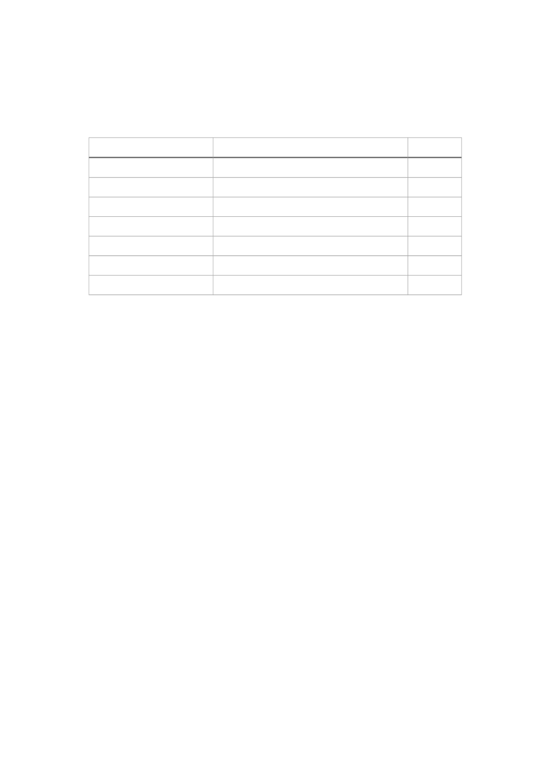
Did you test all input conditions? Were the results as you expected them to be? If you performed your
own test sequence, which tests did you perform and why? The following table is an example of how to
describe your test sequence:
Test stimulus Test motivation Pass/Fail
All inputs 0 Check for stuck-at-1 faults P
All inputs 1 Check for OF P
1 0 0 0 Check for Cry P
1 on INC Adds one to output P
Please comment on the single biggest issue you were facing when simulating the circuit.
Note: I ran into an issue when I originally tested the waveform for the Incrementer. My inputs were in
correct at time 0. Then I noticed that when I created the half adder I tied the connection points “after”
the not gates and not before. Thus my inputs to two of the And gates were incorrect. I had to start
over, redesign my half adder and complete the Incrementer.
Task 1-3: Test the 4-bit Increment Circuit using LEDs on Hardware
Include a picture of your Quartus System Message Window here:
4
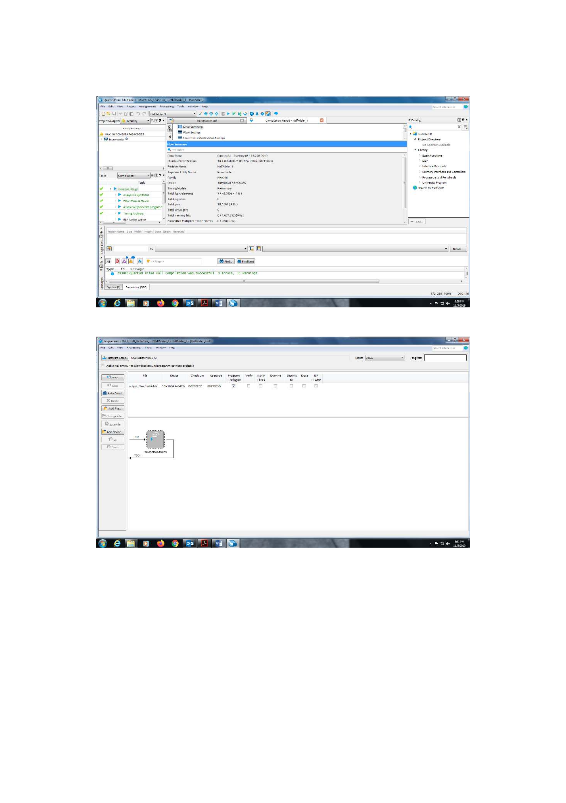
Include a picture of your Programmer Window here:
Was the test on the FPGA board successful?
Yes
What was the biggest issue you were facing when you prepared the design for hardware upload?
5
Reloading driver for board
Record a short video (30 sec – 2 min) showing your circuit working on the hardware kit. Upload the
video to your Google Drive (personal one or ASU one). Copy and paste the sharing link to that video
here. Make sure the link is working and pointing to the correct video. Do NOT upload your video to
YouTube. If your circuit is not working as expected, explain in the video how it is not working and where
you expect the mistake to be from.
Link -bandicam 2019-10-29 17-47-20-963.mp4
At the beginning of your recording, say the task number and circuit name. The
recording needs to be within the time limit. So, be brief in your recording. We
don’t want a 5-min long video.
Task 1-4: Build and Test the 1-Bit Full Adder
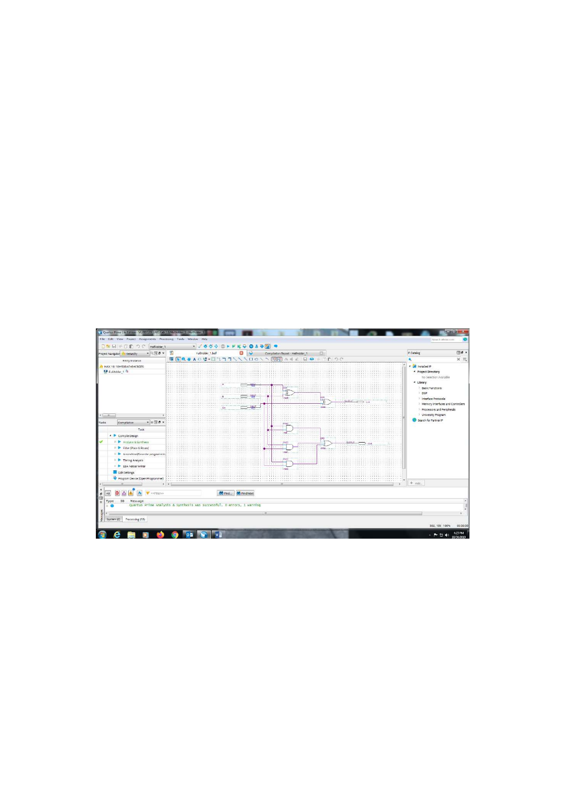
Include a picture of your Quartus circuit here:
Please comment on the single biggest issue you were facing when designing the circuit.
No issues
Include a picture of your Quartus simulation (timing diagram) here:
6
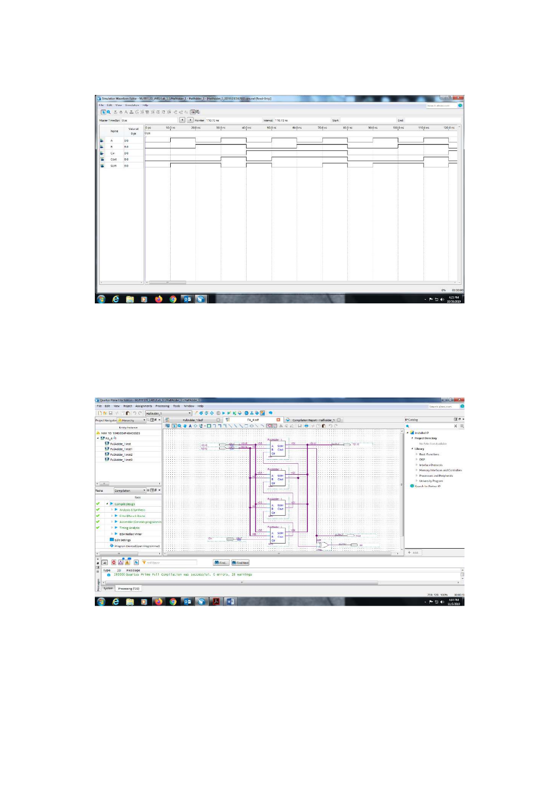
Did the circuit behave as expected? If no, what was wrong? - Yes
Please comment on the single biggest issue you were facing when simulating the circuit. No issues
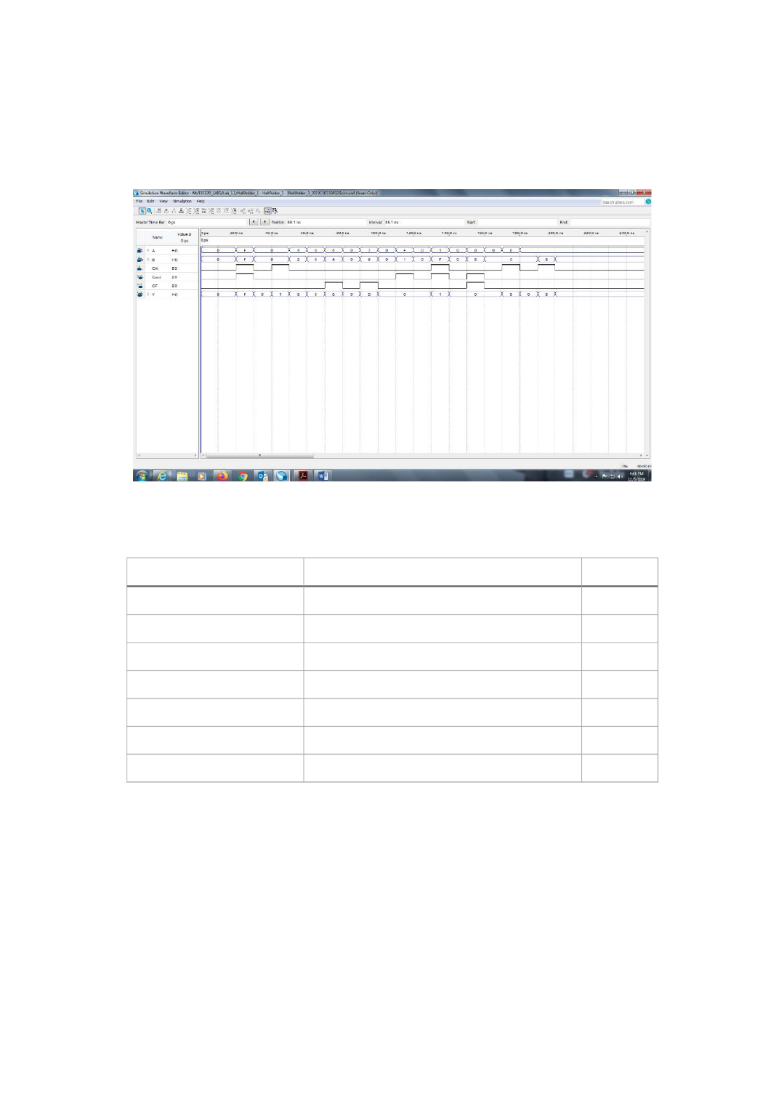
Task 1-5: Build and Test a 4-bit Full Adder- Include a picture of your Quartus circuit here:
Please comment on the single biggest issue you were facing when designing the circuit. - none
7
Include a picture of your Quartus simulation (timing diagram) here:
Which tests did you perform and why? The following table is an example of how to describe your test
sequence. Please add additional columns if you performed more tests. You need to make sure to
perform a sufÏcient number of tests to check the circuit for eventual faults.
Test stimulus Test motivation Pass/Fail
All inputs 0 Check for stuck-at-1 faults P
All inputs 1 and 1 on Cin No change of output but Cout is a 1 P
All inputs 0 and toggle Cin Adds 1 to output P
All inputs 1 Output should be 8 and OF should be high P
Please comment on the single biggest issue you were facing when simulating the circuit.
The OF signal was difÏcult for me.
8
Task 1-6: Test the 4-bit Full Adder using LEDs on Hardware
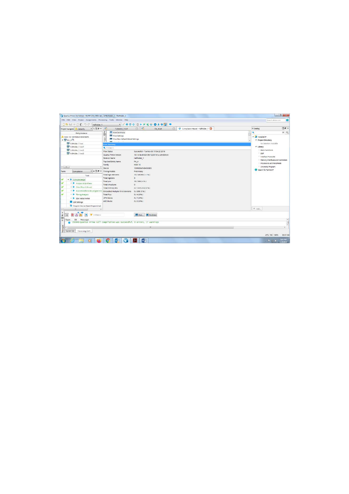
Include a picture of your Quartus System Message Window here:
9
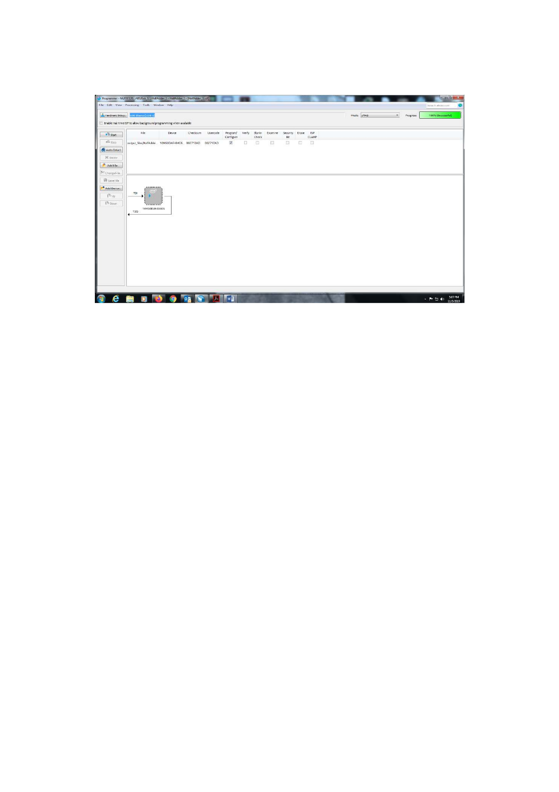
Was the test on the FPGA board successful? - Yes
What was the biggest issue you were facing when you prepared the design for hardware upload?- None.
Record a short video (30 sec – 2 min) showing your circuit working on the hardware kit. Upload the
video to your Google Drive (personal one or ASU one). Copy and paste the sharing link to that video
here. Make sure the link is working and pointing to the correct video. Do NOT upload your video to
YouTube. If your circuit is not working as expected, explain in the video how it is not working and where
you expect the mistake to be from.
Link - bandicam 2019-11-05 17-29-14-602.mp4
At the beginning of your recording, say the task number and circuit name. The
recording needs to be within the time limit. So, be brief in your recording. We
don’t want a 5-min long video. Submit the template to Canvas.
10
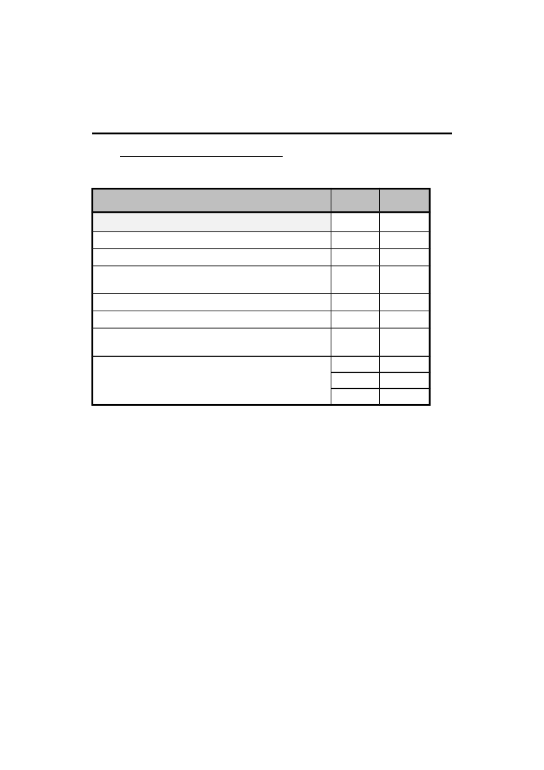
LAB 1: L R G SAB EPORT RADE HEET
Name
Instructor Assessment
Grading Criteria Max Points Points Lost
Description of Assigned Tasks, Work Performed & Outcomes Met
Task 1-1: Build and Test a 1-Bit Half-Adder 5
Task 1-2: Build and Test a 4-Bit Increment Circuit 10
Task 1-3: Test the 4-Bit Increment Circuit Using LEDs on
Hardware + video (10 points included)
20
Task 1-4: Build and Test a 1-Bit Full Adder 5
Task 1-5: Design, Build and Test a 4-Bit Full Adder 10
Task 1-6: Test the 4-Bit Full Adder Circuit Using LEDs on
Hardware + video (10 points included)
20
Points Lost
Lab Score (70 points total) Late Lab
Lab Score
11

