


CSUN COMP 222 Architecture Notes: The Von Neumann Core:
Stored Program and Execution Cycle
Topic: The Core Principles of the Von Neumann Architecture
Context: Stored Program Concept, Instruction Representation, and the Fetch-
Execute Cycle
Part I: A Student’s Foundational Insight into the Von Neumann Model
As a COMP 222 student, my understanding of the Von Neumann architecture is that
it represents the single most significant conceptual leap in the history of computing.
It is the foundational paradigm that moved machines away from being mere
specialized calculators (like the ENIAC, which had to be physically rewired for every
new program) to becoming universal, general-purpose computers.
The architectures core strength lies in its Stored Program Concept. This
revolutionary idea dictates that both the program instructions and the data those
instructions operate on must reside together in the same memory space. This
homogeneity in storage is what allows the machine to treat a program as just
another piece of data, which in turn enables:
Software Flexibility: Programs can be easily loaded, modified, and swapped without
hardware changes.
Self-Modifying Code (Historically): While a dubious practice today, the architecture
originally allowed a program to modify its own instructions, demonstrating the
fluidity between code and data.
Simplified Hardware: A single interface (the System Bus) is needed to interact with
memory for both fetching instructions and manipulating data.
However, this great strength introduces the architectures central flaw: the Von
Neumann Bottleneck. Because the CPU must access the shared memory for both
fetching the next instruction and loading/storing data, the single Data Bus becomes
a massive traffic jam, severely limiting the rate at which the CPU can operate. All of
computer performance engineering since the 1940s has been an elaborate effort to
circumvent this fundamental bottleneck while retaining the elegance of the stored
program principle.
Part II: Formal Definition of the Von Neumann Architecture
The Von Neumann architecture, named after mathematician John von Neumann,
who described its logical structure in 1945, defines the fundamental organization of
almost all modern general-purpose digital computers.
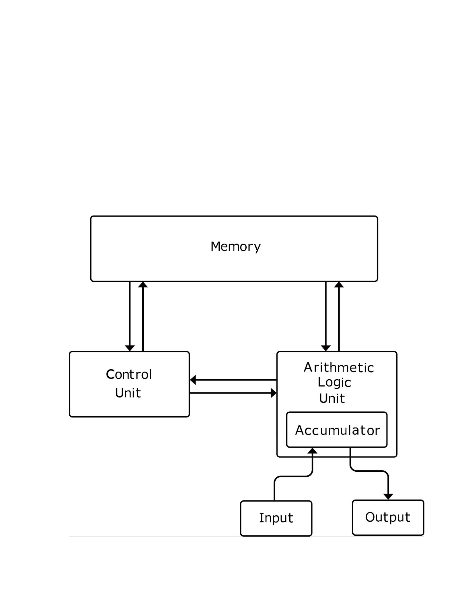
1. The Four Main Components
The model specifies four main structural components connected by a system of
communication pathways (the Bus):
Central Processing Unit (CPU): The "brain" responsible for executing instructions. It
comprises the Control Unit (CU) and the Arithmetic Logic Unit (ALU).
Main Memory: Stores both program instructions and data. Organized as a linear
array of addressable cells.
Input/Output (I/O) Devices: Mechanisms for transferring information between the
computer and the outside world (keyboard, display, disk drives).
System Bus: The communication pathway linking the three major components
(Address Bus, Data Bus, Control Bus).

2. The Stored Program Concept (The Foundational Idea)
The Stored Program Concept is the pillar of the architecture, defining how the
machine operates:
Homogeneous Storage: Instructions are represented as numerical codes (binary)
and stored in memory alongside the data they process. This eliminates the need for
external hardware configuration (like plugboards) to change the program.
Sequential Execution: The CPU executes instructions sequentially, one after the
other, unless explicitly told to jump or branch to a new location by a control flow
instruction.
Central Role of Memory: Memory is not just a passive storage bank; it is actively and
equally accessed for both the operations (instructions) and the operands (data).
3. Instruction Representation
A program is merely a sequence of machine-readable instructions. Each instruction
typically consists of two main parts:
Opcode (Operation Code): Specifies the operation to be performed (e.g., ADD, SUB,
LOAD, JUMP). The Opcode is the critical piece of information that the Control Unit
decodes.
Operand/Address Field: Specifies the data location (memory address, register
number, or immediate value) that the operation will use.
Example: A simple instruction might be represented by a 32-bit word:
Bits 31-26: Opcode (6 bits, allowing
26=64
distinct operations)
Bits 25-0: Address Field (26 bits, allowing a direct address space of
226
bytes)
Part III: The Instruction Execution Cycle (Fetch-Decode-Execute)
The essence of the Von Neumann architecture is the relentless, cyclic process by
which the CPU retrieves, interprets, and carries out instructions stored in memory.
This is universally known as the Instruction Cycle, or the Fetch-Decode-Execute
Cycle. The entire systems performance is governed by the speed and efficiency of
this cycle.
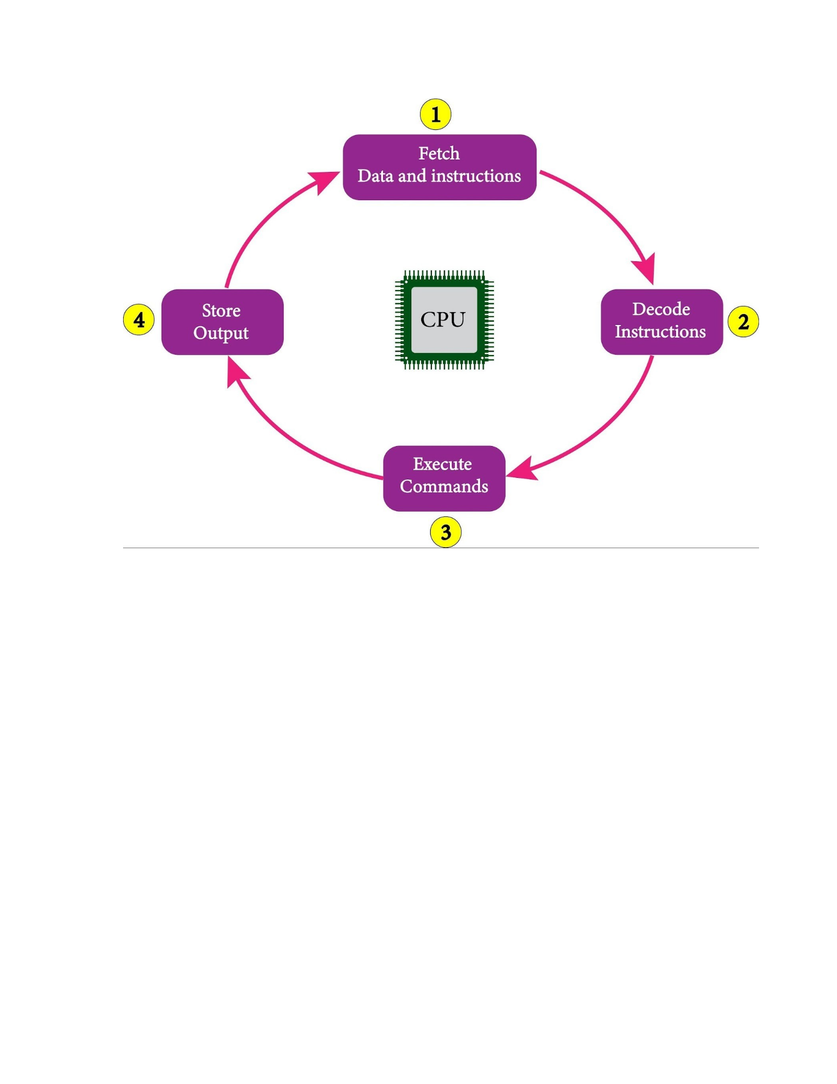
1. Phase 1: The FETCH Cycle (Retrieval from Memory)
The Fetch phase is dedicated to retrieving the next instruction from main memory.
It is a four-step choreography involving the Program Counter (PC) and the memory
interface registers.
A. The Role of the Program Counter (PC)
Function: The PC holds the memory address of the next instruction to be fetched.
Micro-operation 1 (PC
→
MAR): The address contained in the PC is first transferred
onto the Memory Address Register (MAR).
MAR ←PC
System Action: The value in the MAR is then broadcast onto the Address Bus.
B. The Memory Access
Micro-operation 2 (Memory Read): The Control Unit asserts the necessary signals
on the Control Bus (specifically, the
MREQ
―
and
RD
―
signals) to initiate a memory
read operation at the address currently on the Address Bus (the contents of the
MAR).

System Action: The memory controller locates the instruction, and the instruction
word is placed onto the Data Bus (DB).
C. Instruction Latching and PC Update
Micro-operation 3 (DB
→
MBR, PC Update): The CPU latches the instruction from
the Data Bus into the Memory Buffer Register (MBR) (also known as the Memory
Data Register, MDR). Simultaneously, and crucially, the PC is incremented to point to
the address of the next sequential instruction.
MBR ←Memory [MAR]PC←PC+Instruction Size (e.g., 4 bytes)
D. Transfer to Instruction Register (IR)
Micro-operation 4 (MBR
→
IR): The complete instruction, now safely in the MBR, is
transferred to the Instruction Register (IR), where it will be held for the remainder
of the cycle.
IR ←MBR
2. Phase 2: The DECODE Cycle (Interpretation)
Once the instruction is in the IR, the CPU must interpret its meaning. This is the
domain of the Control Unit (CU).
A. Opcode Extraction and Interpretation
Action: The Control Unit extracts the Opcode field (the highest-order bits) from the
IR.
Function: The CU uses combinational logic, often implemented as a large decoder or
a specialized microprogram, to determine two things:
What operation is required (e.g., ADD, LOAD, etc.)?
What addressing mode is used (e.g., direct, indirect, immediate)?
B. Operand Fetch (Data Path Setup)
Action: If the instruction is a memory reference instruction (e.g., LOAD R1,
Address_X), the CU extracts the address field from the IR.
Function: The CU might send this address through the ALU for address calculation
(especially for indexed or relative addressing modes) and place the resulting
effective address back into the MAR. If the instruction is an immediate instruction
(data is part of the instruction), this data is moved directly to the MBR.
MAR ←Address (IR )
3. Phase 3: The EXECUTE Cycle (Action)

This is where the actual computation or data movement occurs, involving the ALU
and general-purpose registers (GPRs).
A. Execution Logic (Varies by Instruction Type)
The steps in the Execute phase are entirely dependent on the Opcode:
LOAD (Data Transfer):
CU asserts
RD
―
and
MREQ
―
at the address in the MAR.
Data is placed on the DB and moved into the MBR.
Data is finally transferred from the MBR to the specified destination register (e.g.,
R1).
R1 ←MBR
ADD (Arithmetic Operation): (Assuming
ADD R1, R2
adds the contents of R2 to R1)
The CU instructs the ALU to perform the addition.
The contents of R1 and R2 are fed into the ALUs input operands.
The ALU performs the operation.
The result from the ALU is stored back into the destination register (R1).
R1 ←R1+R2
JUMP (Control Flow): (An unconditional branch to a new address)
The effective branch address (calculated in the Decode phase) is transferred directly
into the PC, overriding the automatic increment performed in the Fetch phase.
PC←Effective Address
Result: The next Fetch cycle will begin at the new address, changing the programs
flow.
4. Phase 4: The Interrupt Check Cycle
While often omitted in simple descriptions, a crucial step occurs before the CPU
loops back to the Fetch phase: checking for external events.
Action: The Control Unit checks the Control Bus for asserted interrupt request
signals (
∫
―
¿
).
Result (No Interrupt): The cycle begins again at Phase 1 (Fetch), using the updated
PC value.

Result (Interrupt Present): The CPU suspends the normal execution flow, saves the
current PC and register state to the stack, and forces a jump to the Interrupt Service
Routine (ISR) address, effectively hijacking the next Fetch cycle.
Part IV: Detailed Role of Internal CPU Registers
The instruction execution cycle relies entirely on a small set of high-speed registers
within the CPU to hold intermediate values and control state.
1. Program Counter (PC)
Purpose: Instruction sequencing. Always holds the address of the next instruction.
Function in Cycle: Provides the address for the Fetch phase; updated (incremented)
during the Fetch phase; and modified (overwritten) during JUMP or Branch
instructions.
2. Instruction Register (IR)
Purpose: Instruction storage. Holds the current instruction being executed.
Function in Cycle: Receives the instruction word from the MBR during Fetch; its
contents are the input to the Control Unit during the Decode phase.
3. Memory Address Register (MAR)
Purpose: Address holding for bus access. Holds the address that is currently being
broadcast on the Address Bus.
Function in Cycle: Receives the address from the PC during Fetch, or receives the
data address from the CU during Decode/Execute.
4. Memory Buffer Register (MBR)
Purpose: Data/Instruction buffering. Holds the data word being transferred to or
from main memory.
Function in Cycle: Temporarily holds the fetched instruction before it moves to the
IR; holds data being read from memory before it moves to a GPR; or holds data
being written to memory before it moves to the Data Bus.
5. Accumulator (AC) and General Purpose Registers (GPRs)
Purpose: Arithmetic and logical data storage. These hold the operands and results
for the ALU.
Function in Cycle: Provide operands to the ALU during Execute; receive results from
the ALU during Execute.
Part V: The Von Neumann Bottleneck and Performance Implications

The elegant simplicity of the Stored Program Concept—sharing memory for both
instructions and data—is the direct cause of the most significant architectural
performance limitation.
1. The Bottleneck Defined
The Von Neumann Bottleneck refers to the constraint on throughput caused by the
single, shared data path (the Data Bus) between the CPU and main memory.
Problem: The CPU often requires two memory accesses per basic cycle: one to Fetch
the instruction, and a second to Fetch/Store the data operand. These accesses must
occur sequentially over the same Data Bus.
CPU Starvation: A high-speed CPU core often completes internal operations faster
than the bus can supply the next instruction or data word, forcing the CPU to sit idle
and wait.
2. Architectural Solutions to the Bottleneck
Modern architectures do not abandon the Von Neumann model but use complex
techniques to mitigate the bottleneck:
Caches (L1, L2, L3): The primary solution. Instructions and data are copied into
high-speed, local SRAM (Cache) near the CPU. A "hit" in the cache avoids the slow
main memory access entirely. The instruction cache (I-Cache) and data cache (D-
Cache) are often physically separated (a form of limited Harvard architecture within
the CPU).
Pipelining: Overlapping the Fetch, Decode, and Execute phases of multiple
instructions. While Instruction
N
is being executed, Instruction
N+1
is being
decoded, and Instruction
N+2
is being fetched. This maximizes the utilization of the
Data Bus.
Bus Width Expansion: Increasing the Data Bus width (e.g., from 32-bit to 64-bit)
allows more data or a full instruction to be fetched per clock cycle.
Burst Mode: Fetching an entire cache line (e.g., 64 bytes) in one sequence of bus
cycles, rather than one word at a time, to make the single memory request more
efficient.
3. Introduction to the Harvard Architecture Contrast
The theoretical alternative, the Harvard Architecture, uses separate memory spaces
and separate, dedicated buses for instructions and data.
Advantage: Eliminates the Von Neumann Bottleneck entirely, as the CPU can fetch
the next instruction and access the data operand simultaneously.

Usage: Used primarily in embedded systems and Digital Signal Processors (DSPs)
where peak performance and predictable timing are prioritized over programming
flexibility.
Modern Compromise: General-purpose CPUs use a modified Harvard approach
internally (separate I-Cache and D-Cache), but they still share the external bus to
main memory, making them fundamentally Von Neumann machines.
Part VI: Deep Dive into Control Unit and Micro-operations
The transition between the Fetch, Decode, and Execute phases is not magical; it is a
precisely timed sequence of micro-operations orchestrated by the Control Unit (CU)
using the Control Bus.
1. Hardwired vs. Microprogrammed Control Units
The CU itself is responsible for generating the signals that move data between
registers, control the ALU, and assert the bus signals. There are two primary ways to
implement the CU logic:
Hardwired Control: The CU logic is implemented purely through combinational logic
(AND, OR, NOT gates) and sequential logic (flip-flops). Each machine instruction
directly triggers a fixed sequence of electrical signals.
Advantage: Extremely fast execution speed.
Disadvantage: Complex to design, difficult to change (a change to an instruction
requires a hardware redesign).
Microprogrammed Control: The CU logic is stored in a special, fast memory called
the Control Store. Each machine instructions Opcode is an address into the Control
Store, which contains a sequence of micro-instructions. Each micro-instruction is a
low-level command (e.g., Enable_MAR_Write, Assert_RD).
Advantage: Easier to design, flexible (a change to an instruction is just a firmware
change), and supports complex instruction sets (CISC).
Disadvantage: Slower execution due to the micro-instruction fetch phase.
2. The Micro-operation Concept
A micro-operation is the most primitive step that the CPU can perform in one clock
cycle. The entire Fetch-Decode-Execute cycle is merely a sequence of these micro-
operations.
Data Movement: E.g.,
R1 ←R2
(Copy the contents of Register 2 to Register 1).
ALU Operation: E.g.,
R3 ←R1+R2
(Perform addition and store the result).

Control Signal Assertion: E.g., Assert
RD
―
(Place the memory read signal on the
Control Bus).
The instruction execution cycle for even the simplest instruction might involve ten
or more distinct micro-operations, all sequenced and timed by the CU to prevent
resource conflicts and ensure data stability across the buses. For instance, the
timing of Micro-operation 1 (PC
→
MAR) must happen exactly when the Address
Bus is stable and ready to receive the new address.
Part VIII: Architectural and Historical Consequences
The Von Neumann architecture’s principles have dictated the entire trajectory of
computer engineering.
1. The CISC vs. RISC Debate
The Stored Program Concept, particularly the complexity of the Instruction Set
Architecture (ISA), was central to the debate between Complex Instruction Set
Computing (CISC) and Reduced Instruction Set Computing (RISC).
CISC (e.g., Intel x86): Instructions are complex, variable-length, and often perform
multiple micro-operations (e.g., a single instruction might perform a memory read,
an addition, and a result store). This was enabled by Microprogrammed Control
Units.
Consequence: Complex execution cycle, but fewer instructions needed for a given
task.
RISC (e.g., ARM, MIPS): Instructions are simple, fixed-length, and each performs only
one micro-operation (e.g., LOAD, ADD, STORE are separate instructions). This is
enabled by Hardwired Control Units.
Consequence: Simpler and faster execution cycle, but more instructions needed for
the same task.
Modern processors (like x86-64) achieve high performance by dynamically
translating complex CISC instructions into a sequence of simple RISC-like micro-
operations that are executed by a highly pipelined, Hardwired core, blending the
programming convenience of CISC with the execution speed of RISC.
2. The Concept of Self-Modifying Code
The Stored Program Concepts ultimate freedom is allowing programs to modify
their own instructions.
Historical Context: In early assembly language programming, this was sometimes
used to create efficient loops by modifying the operand address of a LOAD or STORE
instruction on the fly.
Modern Prohibition: Today, this practice is strongly discouraged, primarily because:

Security Risk: It is a vector for malicious code to inject itself.
Cache Invalidation: If a program modifies an instruction in main memory, the
Instruction Cache (I-Cache) may hold the old, stale version of the instruction,
requiring complex, costly cache invalidation protocols, which destroy pipeline
efficiency. This is a direct consequence of the shared memory space (Von Neumann
Bottleneck).

