



Digital Logic Study Guide: Core Flip-Flops (SR, JK, D)
Course Context: Digital Logic Fundamentals (Relevant to CSUN
Engineering/Computer Science Electives)
Core Concept: The Flip-Flop as the Fundamental 1-Bit Storage Element
I. Introduction: Sequential Logic and Memory
Digital electronics are broadly classified into two categories: Combinational Logic
and Sequential Logic. Combinational circuits (like adders, multiplexers) produce
outputs based only on the current inputs. Sequential circuits, on the other hand,
produce outputs based on current inputs and the circuits past state (memory).
The flip-flop is the most critical and elementary component of sequential logic. It is a
bistable electronic circuit capable of holding one of two stable states indefinitely,
representing a single binary digit—a 1 or a 0. This capability makes it the
fundamental building block for CPU registers, counters, and RAM (Random Access
Memory).
Key Terminology:
Q and Q-bar (
Q
): The two complementary outputs of the flip-flop.
Q
represents the
stored data bit.
Clock (
Clk
): A periodic square wave signal that synchronizes all state changes
within a digital system.
Edge-Triggered: The circuit only responds to the inputs at the precise rising
(positive) or falling (negative) edge of the clock pulse.
II. The SR Flip-Flop (Set-Reset)
The SR flip-flop (or SR latch, when unclocked) is the most basic memory element. It
can be constructed using two cross-coupled NOR gates or two cross-coupled NAND
gates. We will focus on the Clocked SR Flip-Flop for sequential systems.
2.1 Structure and Operation
The clocked SR FF has two data inputs,
S
(Set) and
R
(Reset), and one clock input,
Clk
. The two main outputs are
Q
(the current state) and
Q
.
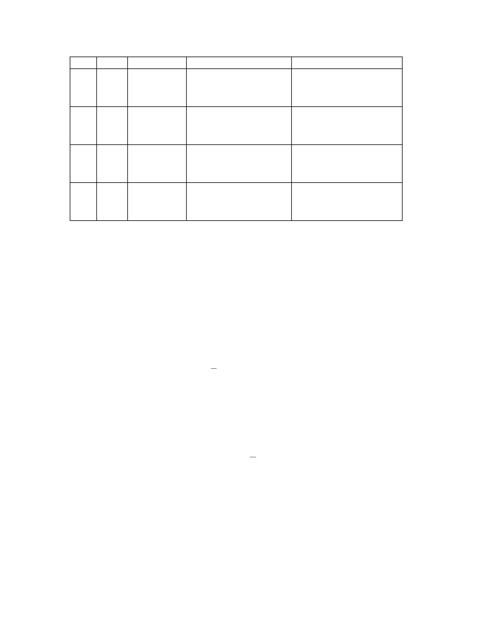
S R Clk Qn+1 State Description
0 0
↑
Qn
Hold (No Change)
0 1
↑
0 Reset (Clear to 0)
1 0
↑
1 Set (Store 1)
1 1
↑
Forbidden / Invalid Ambiguous State
Forbidden / Invalid
Ambiguous State
↑
indicates the state change happens on the rising edge of the clock.
Qn
is the current state;
Qn+1
is the next state.
2.2 Characteristic Equation
The behavior can be summarized by the characteristic equation, which defines the
next state
Qn+1
based on
S
,
R
, and the current state
Qn
:
Qn+1=S+R⋅QnCondition: S⋅R=0
2.3 Personal Insight: The SR Dilemma
Insight: The SR flip-flop perfectly illustrates the trade-off between simplicity and
reliability in circuit design. Its elegance lies in its minimal component count, but its
fatal flaw—the Forbidden State (
S=1, R=1
)—makes it unsuitable for practical,
large-scale systems where unexpected input combinations are inevitable.
If
S=1
and
R=1
simultaneously, both
Q
and
Q
attempt to become 0 (in the NOR-
based latch), which violates the fundamental requirement that they must be
complements. If the inputs return to
S=0, R=0
, the resulting state of
Q
is
unpredictable, depending on minor differences in gate delay times—a phenomenon
known as the Race Condition. System designers must guarantee that this input
combination never occurs, adding complexity to the control logic.
2.4 Common Pitfall: Latch vs. Flip-Flop
Error Analysis: A major point of confusion is the distinction between a Latch and a
Flip-Flop:
Latch: Is level-sensitive. The output can change (is transparent) as long as the
Enable/Clock input is HIGH (or LOW). This makes latches susceptible to race
conditions where inputs change too fast.
Flip-Flop: Is edge-triggered. The output only changes at the precise transition (edge)
of the clock signal. This allows for synchronous operation and effectively isolates the
internal memory from input changes during the majority of the clock cycle,
preventing the transparency issue of latches.
Always remember: When referring to synchronous digital systems (like CPUs), we
are almost exclusively using edge-triggered Flip-Flops.
III. The JK Flip-Flop (Jack Kilby)
The JK flip-flop is considered the "universal" flip-flop because it overcomes the
forbidden state of the SR flip-flop by using internal feedback.
3.1 Structure and Operation
The JK FF has two data inputs,
J
(Set) and
K
(Reset), and includes feedback paths
from the outputs (
Q
and
Q
) back to the input gates. The clock is essential for
synchronous operation.
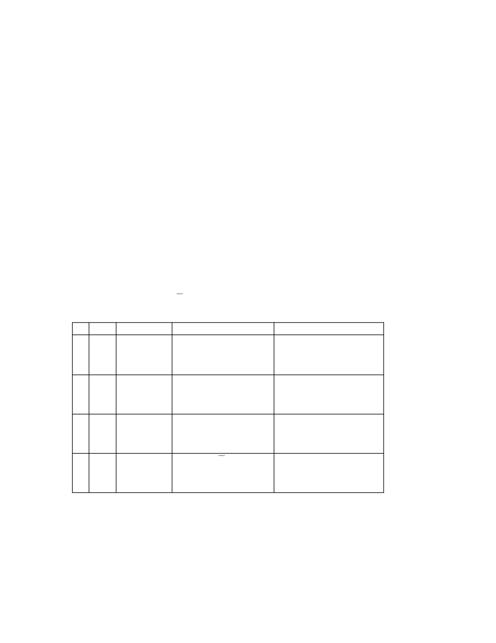
J K Clk Qn+1 State Description
0 0
↑
Qn
Hold (No Change)
0 1
↑
0 Reset (Clear to 0)
1 0
↑
1 Set (Store 1)
1 1
↑
Qn
Toggle (Invert State)
Toggle (Invert State)
3.2 Characteristic Equation
The next state
Qn+1
is defined by:
Qn+1=J⋅Qn+K⋅Qn
3.3 Personal Insight: The Power of Toggling
Insight: The greatest innovation of the JK FF is the Toggle state (
J=1, K=1
), which
acts as a reliable state inversion (
Qn+1=Qn
). This makes the JK FF invaluable for two
specific applications:
Counters: When set to the Toggle mode, a JK FF acts as a simple T (Toggle) flip-flop,
dividing the clock frequency by two. Cascading multiple T FFs creates a ripple
counter or frequency divider.
Simplification: Because the four input combinations are all valid, the JK FF simplifies
the control logic required for state machines compared to the SR FF, which required
external logic to police the forbidden state.
3.4 Common Pitfall: The Race-Around Condition
Error Analysis: While the JK FF solves the SRs forbidden state ambiguity, it
introduces a new problem in the level-sensitive design (latch) called the Race-
Around Condition when
J=1, K=1
.
If the clock pulse is HIGH for too long, the FF toggles once, but the new
Q
and
Q
outputs feed back to the input gates, causing it to toggle again and again while the
clock remains HIGH.
The final state becomes unpredictable because the FF "races around" its feedback
loop multiple times during a single clock pulse.
The Solution (Crucial Point): This is why practical JK flip-flops are Master-Slave
configurations or, more commonly today, Edge-Triggered. Edge-triggering ensures
that the inputs are sampled for only an infinitesimal moment, preventing the output
change from instantaneously becoming the new input, thereby eliminating the race-
around problem.
IV. The D Flip-Flop (Data or Delay)
The D flip-flop is the core 1-bit memory element used in nearly all modern
synchronous digital systems. It is often created from an SR flip-flop by adding a
single inverter between the
S
and
R
inputs and connecting the single data input
D
to
the
S
line.
4.1 Structure and Operation
The D FF has only one data input,
D
. This architecture ensures that
S
and
R
are
always complementary (
S⋅R=0
), thus guaranteeing the exclusion of the forbidden
state from the SR core.
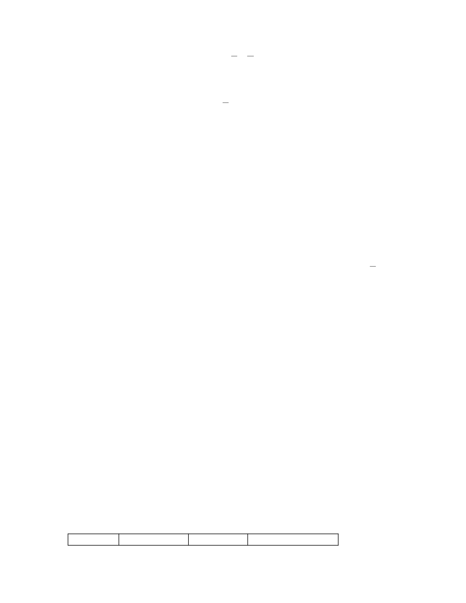
D Clk Qn+1 State Description

0
↑
0 Reset (Stores 0)
1
↑
1 Set (Stores 1)
The operation is simple: Whatever is on the
D
input is stored in
Q
on the next clock
edge. The FF acts like a one-clock-cycle delay element, which is why it is sometimes
called a "Delay" flip-flop.
4.2 Characteristic Equation
The next state
Qn+1
is simply equal to the current data input
D
:
Qn+1=D
4.3 Personal Insight: The Digital Snapshot
Insight: The D flip-flops role is not just to store a bit; its to synchronize the data flow.
When the clock edge arrives, the D FF takes a "snapshot" of the signal on the
D
line,
freezes that value in
Q
, and holds it until the next clock edge. This precise,
synchronized storage allows millions of bits of data to move predictably and reliably
through complex logic circuits like CPUs and memory buses. It provides the
necessary temporal isolation.
4.4 Common Pitfall: Setup and Hold Time Violations
Error Analysis: Since the D FF is highly dependent on the clock edge, two crucial
timing parameters must be respected to guarantee reliable operation:
Setup Time (
tsetup
): The minimum amount of time the data input
D
must be stable
before the active clock edge arrives.
Violation Effect: If
D
changes too close to the clock edge, the FF might not correctly
capture the new data.
Hold Time (
thold
): The minimum amount of time the data input
D
must remain stable
after the active clock edge has passed.
Violation Effect: If
D
changes too soon after the clock edge, it can corrupt the newly
stored data bit.
Crucial Takeaway: Timing violations lead to metastability, a temporary state where
the output
Q
is neither a valid 0 nor a valid 1. This state is highly destructive and
unpredictable, often leading to system crashes. Digital designers spend significant
effort ensuring that signal path delays do not violate these two timing constraints.
V. Summary and Conversion (JK as Universal)
The JK flip-flop is often called "universal" because it can be easily configured to
emulate both T and D flip-flops, as well as the SR operation.
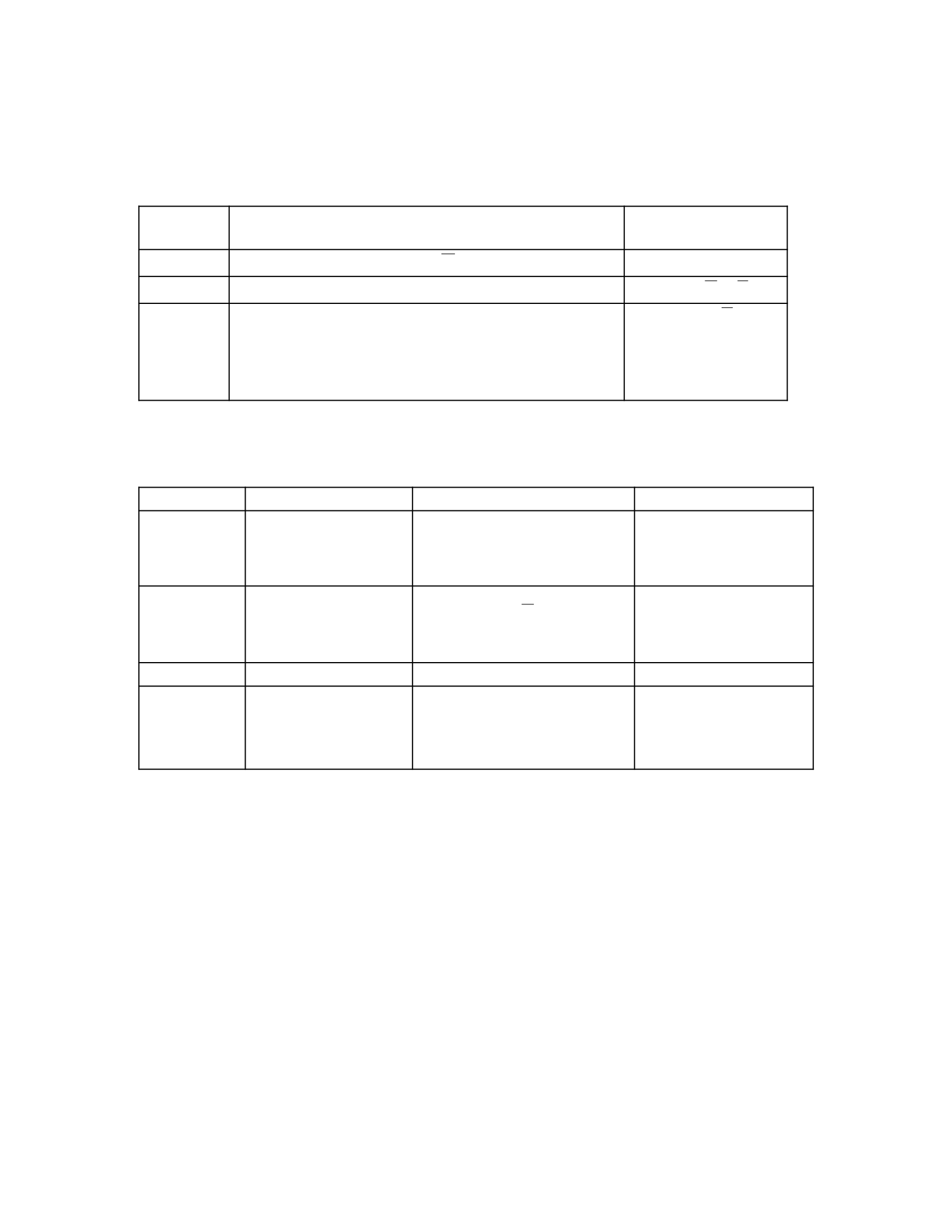
5.1 Flip-Flop Conversion Table
Desired
FF
Configuration (Connect inputs) Next State
Equation
D FF Connect D to J; Connect
D
to K
Qn+1=D
T FF Connect J and K together to T (Toggle input)
Qn+1=T⋅Qn+T⋅Qn
SR FF Connect S to J; Connect R to K (and ensure
S⋅R=0
)
Qn+1=S+R⋅Qn
5.2 Comparative Analysis
Feature SR Flip-Flop JK Flip-Flop D Flip-Flop
Input
Count 2 (
S , R
) 2 (
J , K
)
)
1 (
D
)
Ambiguou
s State YES (
S=1, R=1
)NO (Toggles:
Qn
)NO (Always
Set/Reset)
Function Set/Reset/Hold Set/Reset/Hold/Toggle Data Storage/Delay
Primary
Use
Simple Latches
(not common in
sync. circuits)
Counters, Universal State
Machine
implementations
Registers,
Synchronous Data
Transfer, System
Memory
5.3 Personal Insight: Abstraction in Modern Design
Insight: While the JK flip-flop provides theoretical universality, modern IC design
almost exclusively uses the D Flip-Flop for sequential data storage. Why? Because
the JKs complex Toggle and Set/Reset logic can be easily generated outside the D FF
by simple combinational gates (multiplexers, XOR gates, etc.) that feed the single D
input.
The equation
Qn+1=D
simplifies timing analysis and reduces the complexity inside
the most critical component (the memory cell), making the overall system design
cleaner, more predictable, and faster. The D FF is the optimal building block for
VHDL/Verilog and FPGAs because it is the most efficient representation of a 1-bit
memory cell.

VI. Final Review: The Single Bit of Data
The fundamental importance of these devices cannot be overstated. Every piece of
information—every character on your screen, every calculation in a spreadsheet—is
temporarily held by millions of these tiny circuits.
The D Flip-Flop: The Ultimate 1-Bit Memory Cell
The D flip-flop defines synchronous digital design. Its primary purpose, storing
exactly one bit of data, requires the satisfaction of the following three conditions
simultaneously at the clock edge:
Definition: The FF must correctly sample the
D
input.
Stability: The
D
input must remain stable for the required
tsetup
and
thold
windows.
Synchronization: The new value
Qn+1
must appear only after the clock edge has fully
passed, ready for the next stage of logic to use.
Understanding how a single bit is reliably captured, held, and released via the clock
edge is the key to mastering all advanced topics in computer architecture, from
cache design to pipelining.
Key Takeaways:
SR FF: Simple, but Race Condition is fatal.
JK FF: Solves the Race Condition with Toggling, but often replaced by D FF in
modern ASIC/FPGA design.
D FF: The fundamental memory cell; its reliability hinges on respecting Setup and
Hold Times.
Document End

