

Electronics Lab - AC Models
 wmspikparona
Electronics I and Lab
AC Models
Introduction:
Week 6 lab is based on the AC models of a transistors. After the transistor has been biased with a Q-point near the middle of the load line, we can couple a small AC voltage into the base. This creates an AC collector voltage which is larger than the base voltage and hence this arrangement results in an amplifier with a voltage gain.
Please review the following videos before getting started with this lab:
- Watch the video: “Video 3: Fundamentals of breadboard”
- Watch the video: “Video 4: Basic electrical components”
- Watch the video: “Video 5: Simple resistive circuit with NI myDAQ”
Materials and Equipment:
- Hardware Parts (In the Toolbox):
- An NPN transistor: 2N3904
- Five resistors: Two - 1kΩ, 2kΩ, 10kΩ and 40kΩ
- Three Capacitors: 1μF, 100μF
- Jumper wires
Equipment:
- Software equipment:
- Multisim
- Virtual Instruments (in Multisim)
- Agilent Multimeter
- Hardware Equipment:
- Breadboard
- NI myDAQ Instrument device
- Screw Driver
- Screw Terminal connector
- USB Cable
- Multimeter with probes
- Function Generator, Oscilloscope, Multimeter from NI ELVISmx Intrument Launcher
Procedure:
*** This lab has to be implemented in hardware (using NI myDAQ) as well as Software (Multisim) ***
Part A:
- Analyze the circuit or the amplifier shown in Figure 1. Determine the voltages VB, VE, VC, VBE and VCE. Using the beta value of 100, determine the gain of the amplifier (AV). (Include 20% tolerances for resistors and capacitors).
- Construct the circuit shown in Figure 1 on the breadboard using the hardware parts.
- Using the jumper wires, screw driver and screw terminal connector, connect the board to NI MyDAQ Instrument Device.
- Using the function generator in NI ELVISmx Instrument Launcher, provide the voltage (Vin). Use channel AO0 pin on the NI myDAQ Instrument Device to provide this voltage. Make sure the frequency is 1 KHz frequency.
- Using +15V pin out on the Instrument Device provide the supply voltage VCC.
- Perform the DC Analysis by disconnecting the capacitors and measuring VB, VE, VC, IB, IE and IC.
- Place the capacitors back and using pin AI0 on the NI myDAQ Instrument Device, measure the required voltages: VB, VE, VC VBE, VCE.
- Measure the currents: IC and IE using the Multimeter.
- Use AI1 on the NI myDAQ Instrument Device to measure the load voltage VRL. Record the measurements and compare them with the calculated values in step 1.
- Using the input voltage Vin, base voltage VB and load voltage VRL, determine the gain of the amplifier (AV).
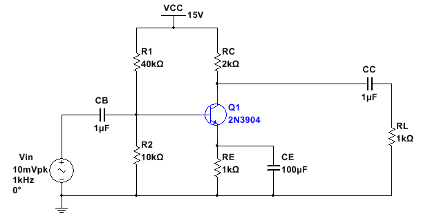
Figure 1
Part B:
- Download the “Lab 6 troubleshooting” file and perform analysis for the circuits to locate the fault embedded in the circuit.
- Step by step measure the key point’s value with Agilent multimeter. Carefully analyze each measured value to locate the fault within the circuits. Fix the fault and with the corrected fault in the newly circuit, measure and record the new values.
Review questions:
- Compare a calculated and measured values. Discuss whether the values are the same of different. If they are different, provide the reasoning.
- Does the DC analysis confirm your calculations?
- What is the gain of the amplifier? Does the gain obtained from analysis match the measured gain? If not, what is the problem and how would you fix it?
- What is the role of capacitors in the AC analysis?
- Did you find any clipping of the collector current? If so, how did you adjust the circuit to avoid clipping?
Deliverables:
- DC and AC analysis of the circuit and all the calculations including gain of the amplifier from step 1.
- Place your student ID card on the breadboard and take a picture of the circuit board and pin out on the NI myDAQ Instrument Device.
- Take screenshots of the measurements obtained from function generator and Oscilloscope and Multimeter on the NI ELVISmx Instrument Launcher on your screen.
- Screenshots of the measurements from DC analysis (without the capacitors). Screenshots of the measurements from AC analysis (with the capacitors). Screenshots of the input voltage Vin, base voltage VB and load voltage VRL.
- Screenshots of collector voltage (Vc) (if any clipping).
- Tabulate the data from analysis and measurements to confirm the gain of the amplifier.
Lab Report:
- Use the Lab report template found in the “Tools and Template” link in the navigation center.
- Include all the deliverables.
- Include all the screenshots of the measurements from circuit design on the breadboard using NI myDAQ Instrument Device and measurements from MI ELVISmx Instrument Launcher.
- Save the document as Lab6YourGID.docx (ex: Lab6G00000000.docx) and submit in Blackboard.
Grading Rubrics
| Grading Criteria | Points |
| Part A: | |
| Analysis of the amplifier circuit in Figure 1 using NPN transistor | 10 |
| Construct the circuit in Figure 1 on the breadboard | 20 |
| Interfacing the breadboard with the NI myDAQ using appropriate pins | 5 |
| DC measurements from the circuit without the capacitors: VB, VE, VC, IB, IE and IC | 5 |
| AC measurements from the circuit with the capacitors using oscilloscope and Multimeter: VB, VE, VC, IB, IE and IC | 10 |
| Measurement of the voltages (Vin, VB and VRL) to compute the gain of the Amplifier | 10 |
| Part B: | |
| Analysis of the circuit in the file “Lab 6 troubleshooting” and find the fault with the circuit | 10 |
| Measurement of new values after the fault is corrected | 10 |
| Review Questions | 10 |
| Report format (Proper use of template) | 10 |
| TOTAL | 100 |
 9 years ago
 20
20
Answer(2)![blurred-text]()
![blurred-text]()
Purchase the answer to view it

 week6_lab_electronics.rtf
Purchase the answer to view it
NOT RATED
- sol_1.zip
Bids(0)