

EE212 week 4 assignment
 sichreq.jplay
Electronics I and Lab
DC Analysis of Transistor and DC Load Line
- For the common emitter circuit shown below (see figure 1) the parameters are:
VBB = 4 V, RB = 220 kΩ, RC = 2 kΩ, VCC = 10 V, VBE(on) = 0.7 V, and β = 200. Calculate the base current (IB), collector current (IC), emitter currents (IE), the VCE voltage and the transistor power dissipation (PT). Show all work.
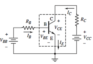
Figure 1
- In the CC circuit shown in Figure 2, calculate the following:
- IB
- IE
- VCE
- VE
- VB. Take β = 49 and VBE = 0.7 V.
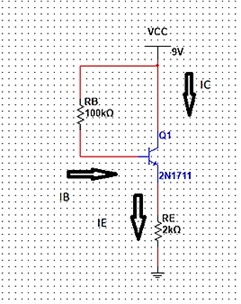
Figure 2
- For the circuit shown in Figure 3 below, draw the DC load line and locate its quiescent or DC working point. Show all work.
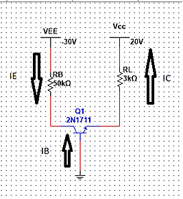
Figure 3
- The data sheet entry that lists how much the power rating of a device has to be reduced is the__________________.
- In a common-emitter circuit, once the base current has been calculated, collector current can be determined by multiplying the base current by ________.
 10 years ago
 5
5
Answer(2)![blurred-text]()
![blurred-text]()
Purchase the answer to view it

NOT RATED
 midterm.rtf
- week4_assignment_1.rtf
- lab_4.docx
Purchase the answer to view it
NOT RATED
- dc_analysis_of_transistor_and_dc_load_line.docx
- week_4_lab_is_based_on_the_fundamentals_of_a_transistor_and_analysis_of_an_analog_circuit..docx
Bids(1)