

DC Analysis of Transistor and DC Load Line
 jav284
For the common emitter circuit shown below (see figure 1) the parameters are:
VBB = 4 V, RB = 220 kΩ, RC = 2 kΩ, VCC = 10 V, VBE(on) = 0.7 V, and β = 200. Calculate the base current (IB), collector current (IC), emitter currents (IE), the VCE voltage and the transistor power dissipation (PT). Show all work.
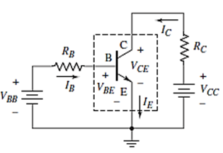
Figure 1
- In the CC circuit shown in Figure 2, calculate the following:
- IB
- IE
- VCE
- VE
- VB. Take β = 49 and VBE = 0.7 V.
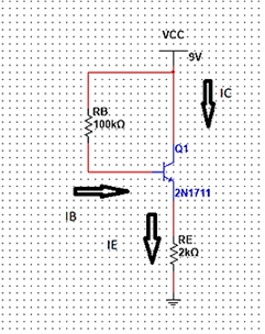
Figure 2
3. For the circuit shown in Figure 3 below, draw the DC load line and locate its quiescent or DC working point. Show all work.
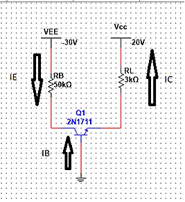
Figure 3
4. The data sheet entry that lists how much the power rating of a device has to be reduced is the__________________.
5. In a common-emitter circuit, once the base current has been calculated, collector current can be determined by multiplying the base current by ________.
**PLEASE SEE ATTACHMENT FOR FIGURES**
 11 years ago
 20
20

Purchase the answer to view it

 e8_e8_e8_dc_analysis_of_transistor_and_dc_load_line.docx
Purchase the answer to view it
- JR produces two types of Tablets (10.1” and 8”), each of which must go through three workstations
- Business DQ
- Burger King was concerned with the sodium intake of its customers and decided to do some analysis of their
- Industrial and Hazardous Waste Question
- Week 2 quiz 100% Correct-SOC/312
- Are women more risk averse in the stock market? A sample of men and women were asked the following question
- read the scenarios below and respond in the form of an essay, which consist of several paragraphs and appropriate priority or task lists. Responses should be supported fully and completely. A well-thought-out response can be accomplished in 300-500 words
- ECO203-Written Assignment 2-3 pages
- Marketing Assignment
- BUS 640 Week 1 Economics of Risk and Uncertainty Applied Problems 2